400-6699-117转1000
咨询列表
上海螣芯电子科技有限公司
您好,欢迎您查看分析测试百科网,请问有什么帮助您的?


| 参考报价: | ¥700000 RMB(人民币) | 型号: | EVG®810 LT+EVG® |
| 品牌: | EVG | 产地: | 奥地利 |
| 关注度: | 61 | 信息完整度: | |
| 样本: | 典型用户: | 暂无 |
400-6699-117转1000
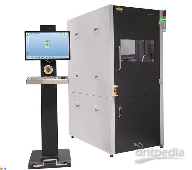
产品描述 EVG®810 LT Features Surface plasma activation for low-temperature bonding (fusion/molecular and intermediate layer bonding) Fastest kinetics of any wafer bonding mechanism No wet processes required Highest bond strength at low temperature annealing (up to 400 °C) Applicable for SOI, MEMS, compound semiconductors, and advanced substrates bonding High degree of materials compatibility (including CMOS) Technical Data "Best Known Method" recipes available for users for the above and for other materials (full list available on request) EVG®301 Features High-efficiency cleaning using 1 MHz megasonic nozzles or area transducers (option) Brush scrubbing for single-side cleaning (option) Diluted chemicals for wafer cleaning Prevents cross-contamination from back to front side Fully software controlled cleaning process Options Pre-bonding station with IR-inspection Tooling for non-SEMI standard substrates echnical DataWafer diameter (substrate size) 50 - 200, 100 - 300 mm LowTemp™ plasma activation chamber Process gases: 2 standard process gases (N2 and O2) Universal mass flow controller: self-calibrating (up to 20.000 sccm) Vacuum system: 9x10⁻² mbar Opening / closing of chamber: automated Loading / unloading of chamber: manual (wafer / substrate placed on loading pins) Optional features Chuck for different wafer sizes Metal ion-free activation Additional process gases with gas mixing High vacuum system with turbo pump: 9x10⁻³ mbar base pressure Material systems that are qualified with LowTemp™ plasma activated bonding Si: Si/Si, Si/Si (thermally oxidized, Si (thermally oxidized)/Si (thermally oxidized) TEOS/TEOS (thermally oxidized) Si/Ge for Germanium-on-Insulator (GeOI) Si/Si3N4 Glass (borofloat, non-alkali): Si/Glas, Glass/Glass Compound semiconductors: GaAs, GaP, InP Polymers: PMMA, Cyclo Olefin Polymers 
SOI键合EVG®810 LT+EVG®301 信息由上海螣芯电子科技有限公司为您提供,如您想了解更多关于 SOI键合EVG®810 LT+EVG®301 报价、型号、参数等信息,欢迎来电或留言咨询。
注:该产品未在中华人民共和国食品药品监督管理部门申请医疗器械注册和备案,不可用于临床诊断或治疗等相关用途

